|
|
 |
Course Programme
Seven courses will be held at the Royal Institute of Technology (KTH) Main
Campus on 1 July, 2007. One course will be held at Stockholm International Fairs
on 2-3 July, 2007.
Course Information (click the link below)
Title:
MRAM, Spin Torque Oscillators and Spintronic Phenomena, 1 July
This course has been cancelled.
Title:
Nanoparticles from the gas phase
This course has been cancelled.
Title:
Nanotribology and nanomechanics and applications to MEMS/NEMS and Bio-MEMS/Bio-NEMS
Time:7 hours
Description and objectives
Nanotechnology undoubtedly is expected to be of major industrial significance.
The nanotechnology is still in its infancy and the emphasis to date has been on
the fabrication and laboratory demonstration of individual components. The field
of MEMS/NEMS has expanded considerably over the last decade. Micro/Nanosystems
have begun to be commercially used. MEMS/NEMS devices are produced by various
lithographic and nonlithographic fabrication processes. Silicon-based MEMS/NEMS
devices are made from single-crystal silicon, LPCVD polysilicon films and other
ceramic films. For high temperature applications, SiC and other films are being
developed to replace polysilicon films. There are bioadhesion issues in BioMEMS/BioNEMS
which need to be addressed. Tribology of various devices which require relative
motion is of importance.
The scale of operation and large surface-to-volume ratio of the devices
result in very high retarding forces such as friction and adhesion that
seriously undermine the performance and reliability of the devices. These are
tribological phenomena that need to be studied and understood at the micro- to
nanoscales. In addition, materials for these devices must exhibit good micro/nanoscale
tribological and mechanical properties. There is a need to develop lubricants
and identify lubrication methods that are suitable for these devices.
Measurement and evaluation of mechanical properties of micro/nanoscale
structures is essential to help address reliability issues. Using atomic force
microscopy-based techniques, researchers have conducted micro/nanotribological
studies of materials and lubricants for use in these devices. Mechanical
properties of nanoscale structures have also been measured. In addition,
component level testing has also been carried out to aid in better understanding
of the observed tribological phenomena in these devices. A fundamental
understanding of nanoscale tribology and mechanics of MEMS/NEMS and BioMEMS/NEMS
is essential as these devices proliferate in the marketplace.
This course provides an introduction to Principles of Nanotribology and
Nanomechanics followed by Applications to MEMS/NEMS and BioMEMS/BioNEMS.
Content
I. Principles of Nanotribology and Nanomechanics
- Introduction to Tribology
Overview of Surface Roughness, Adhesion, Friction, Interface
Temperatures, Wear, and Lubrication
- Nanotribology, Nanomechanics and Material Characterization Studies Using
Scanning Probe Microscopy
Overview of Surface Imaging, Adhesion, Friction, Scratching, Wear,
Indentation/Localized Deformation/Nanofabrication, and Lubrication
II. Adhesion and Stiction
- Introduction
- Mechanisms of Solid-Solid Adhesion
- Mechanisms of Liquid Mediated Contact
- Adhesion Measurement Techniques
- Lubrication Approaches and Typical Stiction Data
- Examples of Methods to Reduce Adhesion and Stiction in Magnetic Storage
Devices and MEMS/NEMS
III. Applications to MEMS/NEMS and BioMEMS/BioNEMS
- Introduction
Definition of MEMS/NEMS and characteristic dimensions
Examples of MEMS/NEMS and BioMEMS/BioNEMS with Tribological Issues
Importance of Mechanics of Nanostructures
- Nanotribological Studies of MEMS/NEMS Materials and Lubricants
- Bioadhesion Studies
- Nanopatterned Surfaces for Superhydrophobicity
- Device Level Studies
- Mechanics of Nanostructures
Course materials: Copies and a CD
of all slides in the PowerPoint format will be provided before the class.
Recommended text book: Bhushan, B., Nanotribology and Nanomechanics An
Introduction, Springer-Verlag, Heidelberg, Germany, 2005.
Instructor: Bharat Bhushan, prof,
Ohio State University, Columbus
 Dr.
Bharat Bhushan is an Ohio Eminent Scholar and The Howard D. Winbigler Professor
in the Department of Mechanical Engineering, a Graduate Research Faculty Advisor
in the Department of Materials Science & Engineering, and the Director of the
Nanotribology Laboratory for Information Storage & MEMS/NEMS (NLIM) at the Ohio
State University, Columbus, Ohio. He holds two M.S., a Ph.D. in mechanical
engineering/mechanics, an MBA, and three semi-honorary and honorary doctorates.
His research interests are in nanotribology and nanomechanics and their
applications to magnetic storage devices and MEMS/NEMS (Nanotechnology). He has
authored 5 technical books, more than 70 handbook chapters, more than 600
technical papers in referred journals, and more than 60 technical reports,
edited more than 40 books, and holds 16 U.S. and foreign patents. He is
co-editor of Springer NanoScience and Technology Series and Microsystem
Technologies Micro- & Nanosystems and Information Storage & Processing Systems
(formerly called Journal of Information Storage and Processing Systems). He has
organized various international conferences and workshops. He is the recipient
of numerous prestigious awards and international fellowships. He is a member of
various professional societies, including the International Academy of
Engineering (Russia). Dr.
Bharat Bhushan is an Ohio Eminent Scholar and The Howard D. Winbigler Professor
in the Department of Mechanical Engineering, a Graduate Research Faculty Advisor
in the Department of Materials Science & Engineering, and the Director of the
Nanotribology Laboratory for Information Storage & MEMS/NEMS (NLIM) at the Ohio
State University, Columbus, Ohio. He holds two M.S., a Ph.D. in mechanical
engineering/mechanics, an MBA, and three semi-honorary and honorary doctorates.
His research interests are in nanotribology and nanomechanics and their
applications to magnetic storage devices and MEMS/NEMS (Nanotechnology). He has
authored 5 technical books, more than 70 handbook chapters, more than 600
technical papers in referred journals, and more than 60 technical reports,
edited more than 40 books, and holds 16 U.S. and foreign patents. He is
co-editor of Springer NanoScience and Technology Series and Microsystem
Technologies Micro- & Nanosystems and Information Storage & Processing Systems
(formerly called Journal of Information Storage and Processing Systems). He has
organized various international conferences and workshops. He is the recipient
of numerous prestigious awards and international fellowships. He is a member of
various professional societies, including the International Academy of
Engineering (Russia).
Title:
Introduction to Scanning Probe Microscopy - STM
Time: 6 hours
Description and objectives
This course is intended to give an overview about nanoparticles suspended in a
gas phase, aerosols, their main properties, fabrication techniques and
applications. The attendee will learn about the fundamentals of aerosol science
and technology and about the great possibilities as well as the limitations of
generation nanoparticles from the gas phase.
Content
- Introduction to surface and nano science.
- Basic principles of STM and AFM
Tunneling, force measurements and image formation
Modes of operation for STM and AFM
- Experimental set-up
- Structural and electronic information from an image.
What can we learn and what are the limitations?
Theoretically generated images
Diffusion barrier from STM-videos
- Tunneling spectroscopy
Capturing the electronic structure on a nanometer scale
Single molecule characterization
Course materials: Lectures notes
and reprints supplied by the instructor
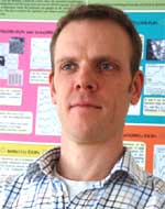
Instructor: Mats Göthelid, PhD, Royal
Institute of Technology
 Doc
M. Göthelid research concerns atomic and electronic structure of surfaces and
surface reactions using scanning probe microscopy and different types of
electron and X-ray spectroscopy. He has been teaching Surface Physics for more
than 10 years. Doc
M. Göthelid research concerns atomic and electronic structure of surfaces and
surface reactions using scanning probe microscopy and different types of
electron and X-ray spectroscopy. He has been teaching Surface Physics for more
than 10 years.
Title:
Ion scattering techniques and secondary ion mass spectrometry for material
analysis
This course has been cancelled.
Title:
Chemical routes to thin films
This course has been cancelled.
Title:
High Resolution Analytical Microscopy of Nanomaterials and Thin Films
Time: 6 hours
Description and objectives
The properties of nanomaterials and thin films are governed by the fine scale
microstructure. Therefore, it is important to extract information on the atomic
scale. This course will give an overview of the abilities of atom probe and
electron microscopy techniques to characterize the microstructure and
microchemistry of materials with high resolution. Recent developments of the
microscopy techniques of atom probe (AP), focused ion beam (FIB), scanning
electron and transmission electron microscopy (SEM and TEM) will be covered.
Examples of applications in nanostructures and thin films will be presented.
Content
SEM and FIB part (Mats Halvarsson):
- Basic principles of electron and ion optics
- Instrumentation
- Image formation
- Contrast mechanisms in different imaging modes
- Energy Dispersive X-ray analysis (EDX)
- n-situ ESEM experiments
AP part (Krystyna Stiller)
- basic principles of: .
a) imaging in AP
b) chemical analysis in AP
- 3-dimensionel AP
- Advantages and limitations of AP- technique
- Specimen preparation
- Examples of applications
TEM (Eva Olsson)
- Basic principles of transmission electron microscopy (TEM) and scanning
TEM (STEM)
- Instrumentation
- Image formation
- Contrast mechanisms in different imaging modes
- Electron diffraction
- Energy Dispersive X-ray analysis (EDX)
- Electron Energy Loss Spectroscopy (EELS)
- In-situ dynamic experiments
Course materials: Copies of
powerpoint presentations.
Instructors:
PhD. Mats Halvarsson, Prof. Eva Olsson and Prof. Krystyna Stiller work in the
group for Microscopy and Microanalysis at Chalmers University of Technology in
Sweden. The general aim of the research of the group is to understand how the
microstructure of materials (down to single atoms) influences their properties.
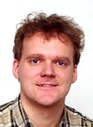 Mats Halvarssons main research tools are electron and ion microscopes and their
add-on equipment. His research concerns hard, wear protective coatings produced
by Chemical Vapour Deposition (CVD) and high temperature corrosion of materials
such as Fe-Cr stainless steels, molybdenum disilicides and Fe-Cr-Al alloys. Mats Halvarssons main research tools are electron and ion microscopes and their
add-on equipment. His research concerns hard, wear protective coatings produced
by Chemical Vapour Deposition (CVD) and high temperature corrosion of materials
such as Fe-Cr stainless steels, molybdenum disilicides and Fe-Cr-Al alloys.
 Eva
Olsson is mainly using advanced analytical microscopy to characterize the
functional microstructure of materials including the characterization of
structure and properties of individual defects. The interfaces are of particular
interest due to their significant influence on properties and microstructural
evolution. The goal is to formulate models with which the physical properties
can be predicted and new devices tailored. The main research tool is analytical
transmission electron microscopy and scanning probe techniques. The research
activities include bulk and thin film oxides (e.g. ZnO, YBa2Cu3O7-x, SrTiO3, Al/AlOx/Al
barriers, La0.67Sr0.33MnO3), photoactive nanostructures (e.g. gold and silver
nanoparticles), magnetic nanoparticles and carbon nanotubes. The research spans
from fundamental research to applied research in collaboration with industry. Eva
Olsson is mainly using advanced analytical microscopy to characterize the
functional microstructure of materials including the characterization of
structure and properties of individual defects. The interfaces are of particular
interest due to their significant influence on properties and microstructural
evolution. The goal is to formulate models with which the physical properties
can be predicted and new devices tailored. The main research tool is analytical
transmission electron microscopy and scanning probe techniques. The research
activities include bulk and thin film oxides (e.g. ZnO, YBa2Cu3O7-x, SrTiO3, Al/AlOx/Al
barriers, La0.67Sr0.33MnO3), photoactive nanostructures (e.g. gold and silver
nanoparticles), magnetic nanoparticles and carbon nanotubes. The research spans
from fundamental research to applied research in collaboration with industry.
 Krystyna
Stiller is especially interested in investigations of processes of phase
transformations and high temperature oxidation. Special emphasis of her research
is put to studies of the microstructure and composition of thin surface layers
and grain boundaries. In her studies she uses both transmission electron
microscopy and atom probe analysis. The last mentioned technique enables
investigations of variation in material chemistry on a sub-nanometer scale with
equal sensitivity for all elements. Krystyna Stiller has contributed to the
development of the technique and its applications. She is working closely with
the Swedish industry. Krystyna
Stiller is especially interested in investigations of processes of phase
transformations and high temperature oxidation. Special emphasis of her research
is put to studies of the microstructure and composition of thin surface layers
and grain boundaries. In her studies she uses both transmission electron
microscopy and atom probe analysis. The last mentioned technique enables
investigations of variation in material chemistry on a sub-nanometer scale with
equal sensitivity for all elements. Krystyna Stiller has contributed to the
development of the technique and its applications. She is working closely with
the Swedish industry.
Course Programme at the Stockholm International Fairs, 2-3 July
Title: X-Ray
Photoelectron Spectroscopy (XPS/ESCA)
Time: 2 days, Monday and Tuesday
(09:00 to 17:00)
Description and objectives
Scientists, engineers, students, and technicians who would like a detailed
understanding of the use of XPS/ESCA for surface analysis should attend this
course. Learn about optimizing the analysis of surfaces with x-ray photoelectron
spectroscopy, approaches for qualitative and quantitative analysis, the types of
problems that can be solved with XPS/ESCA, and the latest developments in
instrumentation.
Content:
Day 1:
- Introduction terminology, surfaces, types of surfaces. 0.5 hour
- The principles of XPS production of photoelectrons, peak labeling,
electronic figuration of atoms, atoms, molecules, solids, energy, spectra,
Auger process, valence spectra, handbooks, books, surface sensitivity,
information depth, sample handling, spin-orbit splitting, chemical shift,
plasmons, multiplet splitting, shake-up. 3 hours
- Instrumentation dual anode, Bremsstrahlung, monochromatic source,
electron energy analyzers, spectrum acquisition, energy resolution,
scattering in analyzers, electron detectors, pulse counting, position
sensitive detectors, small area analysis, area location, imaging XPS,
methods, equipment and examples, vacuum system, samples, energy scale
calibration. 3.5 hours.
Day 2:
- Qualitative analysis identification of elements, changing x-ray
sources, charging, interpretation of chemical shift, relaxation effects,
Auger parameter, peak widths, lineshapes. 2 hours
- Quantitative analysis sensitivity factors, ionization cross section,
asymmetry parameter, analyzer transmission, reference spectra, intensities,
background subtraction, detection limit, effect of thin overlayers. 2 hours
- Artifacts x-ray damage, charging, methods for charge control, ghost
peaks. 0.5 hour
- Data acquisition and processing processing data, Tougaard background
subtraction, satellite subtraction, peak area, lineshapes, curve fitting,
deconvolution. 1 hour
- Depth profiling non-destructive and destructive methods, angle
resolved XPS, diffraction, elastic scattering, thickogram, inelastic loss
method, sputtering, depth calibration. 2 hours
- Applications some further examples of applications of XPS. 0.5 hours
- Instrument selection and summary factors to consider, general summary.
0.2 hours.
Course materials: Course notes
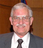
Instructor: PhD John T. Grant,
Distinguished Research Scientist, University of Dayton.
 John
T. Grant has more than 35 years of experience in the field of surface science.
His current interests include all forms of surface analysis, particularly
electron spectroscopies, see:
www.surfaceanalysis.org John
T. Grant has more than 35 years of experience in the field of surface science.
His current interests include all forms of surface analysis, particularly
electron spectroscopies, see:
www.surfaceanalysis.org
Registration Fee for Courses
The cost for participating in the course programme at KTH main Campus on 1
July is:
| Registration fee for Courses 1 July |
Excluding VAT |
Including VAT |
| Early registration fee, until 25 April |
2 000 SEK |
2 500 SEK |
| Late registration fee, after 25 April |
2 500 SEK |
3 125 SEK |
You pay the registration fee once and you are then allowed to attend all courses
in the course programme on the 1 July. Please follow the payment
instructions carefully on the Payment page.
The cost for participating in the course programme on 2-3 July at Stockholm
International Fairs is:
| Registration fee for Course 2-3 July |
Excluding VAT |
Including VAT |
| Early registration fee, until 25 April |
3 000 SEK |
3 750 SEK |
| Late registration fee, after 25 April |
3500 SEK |
4 375 SEK |
Please follow the payment instructions carefully on the Payment page.
Swedish tax legislation requires participants to pay their registration fee
either including or excluding Swedish VAT. Therefore, please identify your
category below and choose the appropriate alternative on the registration form.
Alternative 1: Including VAT
- Registration fees paid by non-taxable entities
(institutions/organisations etc) and private persons within the
European Union.
- All registration fees paid by participants or companies within
Sweden.
- All registration fees for accompanying persons.
Alternative 2: Excluding VAT
- Registration fees paid by companies and other taxable entities (also
including taxable institutions/organisations) within the European
Union, except from Sweden. Please note that according to Swedish law,
your company VAT No. must be stated on your registration form.
- Alternative 3: Excluding VAT
- All registration fees paid from countries outside the European
Union
Swedish participants must always pay the registration fee including
VAT. Hotels, social events and fee for accompanying persons must always
be paid including VAT. Please note that Sweden is not a member of the
European Monetary Union.
|
To on-line registration please
click here.
|
|